The Rising Demand for HDI PCBs
Fueled by AI Servers and High-Speed
Networking
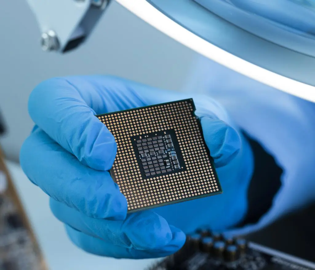
The world of printed circuit boards (PCBs) is undergoing a significant transformation, driven by rapid advancements in technology—particularly in AI servers, high-speed networking, and mobile devices. High-Density Interconnect (HDI) PCBs, known for their ability to pack more connections into compact, high-performance packages, are seeing unprecedented demand. According to recent industry data, HDI PCB demand has surged by 10.4%, reflecting the growing need for cutting-edge solutions in a world increasingly dominated by artificial intelligence (AI) and data storage.
HDI PCB Demand Growth: AI Servers and High-Speed Networking at the Forefront
The exponential rise of AI technology, especially the deployment of AI servers and high-speed networking infrastructure, is a key driver of HDI PCB market growth. These servers require extremely high processing power, memory bandwidth, and efficient heat dissipation—all of which place significant demands on PCB design.
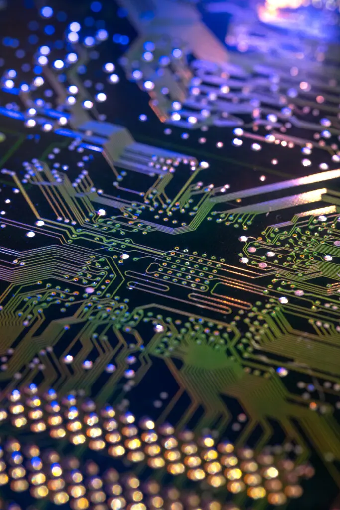
HDI PCBs meet these challenges by enabling ultradense interconnection between
components, while maintaining signal integrity and managing impedance across
complex layer stacks. For instance, a typical server PCB must support the integration of
CPUs, GPUs, storage drives, and multiple high-speed network interfaces—all within
compact form factors. This requires not only HDI architecture but also high-TG (glass
transition temperature) materials, precise stack-up planning, and advanced via structures such as via-in-pad or laser microvias to optimize electrical performance.
As AI-powered applications – like autonomous driving, real-time diagnostics, and generative machine learning – scale in complexity, so does the need for PCBs that can support low-latency, high-throughput data processing.
HDI technology is not just a preference; it has become a technical necessity.
Mobile Phones: A Shift in PCB Usage
Historically, mobile phones were the primary consumers of HDI PCBs, accounting for 61% of the market in 2015. However, this figure has declined to 46% in 2025, reflecting the diversification of HDI applications across multiple industries.
While smartphones still demand compact, multilayered PCBs for advanced features like 5G connectivity, facial recognition, and high-definition cameras, manufacturers are now relying on more cost-optimized and mature PCB technologies in mid-range models. In contrast, industries like AI and cloud computing are now the driving force behind the push for more advanced PCB architectures.

Server Data Storage: A Steady Increase in Demand
Server-based data storage has emerged as another significant growth area for HDI PCBs. In 2015, servers accounted for only 3.4% of HDI PCB demand. By 2025, this figure is projected to rise to 10.5%. This surge mirrors the explosion of global data, driven by IoT, video streaming, edge computing, and large-scale AI model training.
Designing PCBs for modern server storage is a complex task. These PCBs must support high-speed interfaces like PCIe Gen 5, DDR5 memory, and NVMe SSDs, while minimizing signal loss, crosstalk, and thermal stress. As a result, engineers increasingly favor HDI stack-ups that incorporate buried/blind vias, sequential lamination, and high-speed signal routing across controlled-impedance layers.
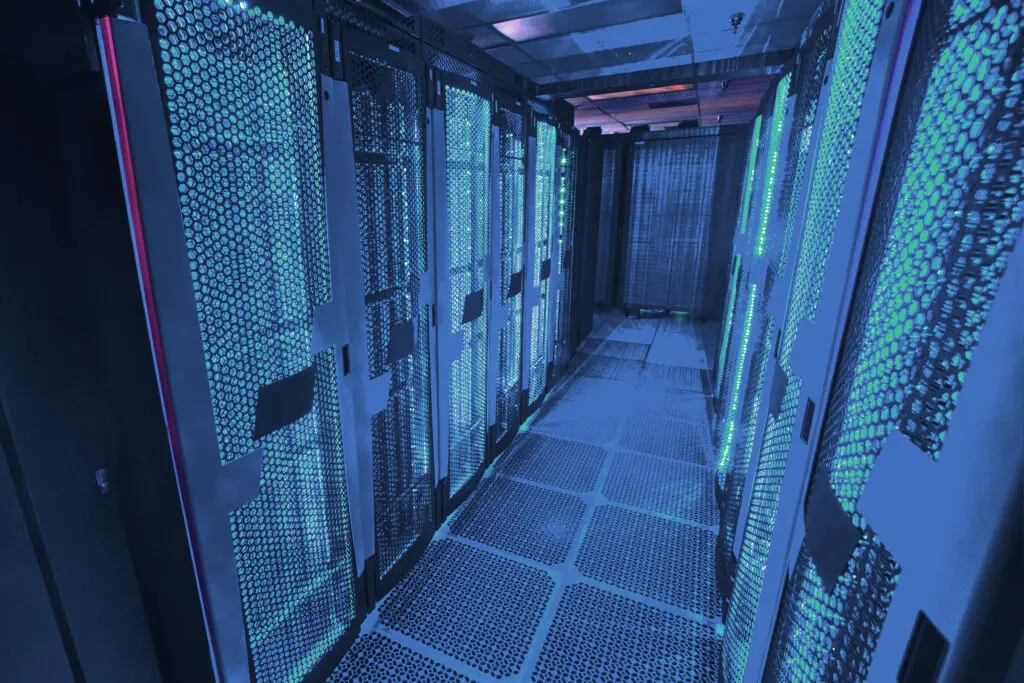
Additionally, server boards must withstand continuous operation in thermally challenging environments. Therefore, material selection becomes a more important factor: FR4 may be insufficient, making way for advanced laminates like polyimide or high-frequency materials with low dielectric loss.
The Rise of Multi-Layer PCBs: A 41.7% Growth in High-Layer Count Designs
Another key trend is the rising demand for multi-layer PCBs, particularly those with 18 layers or more, a segment forecast to grow by 41.7% from 2024 to 2025. These complex PCBs are integral to AI servers and high-speed optical modules, where routing density, signal isolation, and power integrity are paramount.
In high-layer count PCBs, careful planning of the layer stack-up is key to maintaining signal quality. Techniques such as differential pair routing, ground-signal-ground layer configurations, and impedance matching are employed to handle high-speed data without degradation.
Moreover, designers often incorporate embedded capacitors and power planes to reduce noise and enhance power delivery across the board. Optical modules, used for long-distance high-speed data transmission, also rely on high- precision PCBs to support laser drivers, photodetectors, and transceiver ASICs. Any design flaw in such systems can result in data errors or signal distortion at high frequencies, underscoring the need for meticulous PCB engineering.
The Future of HDI PCBs: A Key Enabler of Technological Advancements
Looking ahead, HDI PCBs will continue to play a pivotal role in enabling advanced technologies across multiple industries. From quantum computing to 5G infrastructure and autonomous systems, the demand for compact, high-performance PCB designs will only intensify.
To remain competitive, PCB manufacturers must not only meet today’s performance
standards but also anticipate tomorrow’s needs. This includes integrating newer
materials, tighter tolerances, and design-for-manufacturing (DFM) principles early in the
product development cycle.
In conclusion, the HDI PCB market is entering a new era—driven by AI servers, high-speed networking, and data-centric applications. With a 10.4% growth forecast and increasing demand for multi-layer and data server solutions, HDI PCBs are set to remain a cornerstone of innovation in electronics for years to come.