PCB Design : Cost optimize your design and specifications
In a fast-spinning world of electronics with a constant pursuit of cost reductions and profit optimization, it might be time to take and see if your PCB design, specification and drawings contribute to the case or if it needs a 360° review.
Knowledge is the key to identify the small detail that makes the big cost difference for your Printed Circuit Board. There are many different types of PCB and multiple choices to be made between the development of Schematic and BOM to PCB technology selection, electronic PCB design, mechanical & physical properties, and PCB specification.
Component technology and BGA size
The component size and technology have the most significant influence on the PCB cost.
Most surface-mounted microchips can be designed into standard PCBs with plated through holes. If the same microchip comes in a BGA package, it might need micro-via & buried vias using a higher wiring density to be designed into an HDI PCB.
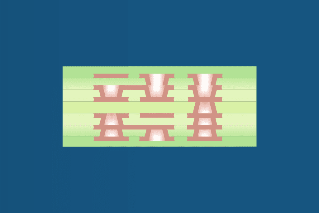
Generally speaking, PCBs containing BGAs become HDI PCBs when the ball center to center-to-center pitch is below 0,8mm. If your physical board properties allow it and the component availability is equal, you should strive to find the BGA with the largest pitch to reduce the component and PCB cost.
Example: The same BGA microchip can be found with pitch 0,8mm, 0,6mm, and 0,5mm. The 0,8mm pitch BGA can be routed on an 8-layer standard PCB with a price index of 100. The 0,6mm pitch can be routed on a (1-6-1) 8 Layer 1 step HDI PCB with a price index of 200. The 0,5mm pitch BGA can be routed on a (2-4B-2) 8 Layer 3 step HDI PCB with a price index of 350.
The number of lamination steps is the most significant cost driver for HDI and Ultra HDI PCBs. Designs with BGAs ≤0,4mm and multiple rows challenge the capability of HDI suppliers, which lead to the use of Ultra HDI design parameters, reducing availability and increasing the cost.
PCB Material selection
Correct material selection complying with the performance and functionality of your application also plays a crucial role in the PCB cost.
Most common stack-ups of standard PCBs are specified with 35µm Cu on all layers. Then the manufacturer starts on 17,5µm Cu on outer layers and 35µm Cu on inner layers, since the final outer layer Cu thickness reaches approximately 35µm after plating. But 35µm Cu on the inner layers isn’t always required and can be replaced by 17,5µm for the current flowing in many electronic devices which in turn lowers costs.
Beyond this, Cu thickness above standard 35µm represents a considerable extra cost.
The base material choice depends on the PCB technology used for your application and the performance needed. By specifying a specific brand and type of material you will diminish the supplier availability and often prolong the lead-time of the suppliers by adding additional material purchase time.
Seeking advice on the material specification from a specialist like ICAPE Group can save time and money by ensuring that your choices are based on performance rather than a specific brand and type of material. We recommend specifying the important critical material characteristics for the performance of your application like: Tg. Temperature Grade, CTE Coefficient of Thermal Expansion, Dk Dielectric Constant & Df Dissipation Factor, CTI Comparative Tracking Index, MOT Max Operating Temperature, etc.
Thereby you allow the supplier to provide their offer based upon the most available and cost-optimized material fulfilling your specified criteria.
PCB Thickness and Stack-up
Standard Stack-ups contain only 1 sheet of prepregs in between each conductive layer. Using two or more sheets of prepreg will increase the PCB cost by approximately 2,5-6 USD/m² per sheet.
The most common PCB thickness is 1,6mm, but could the thickness be reduced to 1,0mm or 0,8mm without compromising the mechanical or electrical performance? Reducing the thickness can provide direct cost savings on the PCB price of 1-2 USD/m², but it also reduces the weight leading to large cost savings on the freight and finally it will reduce the weight of your application.
Panel design & PCB separation
The PCB suppliers are using standard-size production panels between 18×24” to 21×26” but some of the newest factories are going up in double-size production panels like 28×49” to optimize the production cost. Most PCBs are delivered in a customer-defined delivery panel designed to optimize the assembly cost. The optimization for the supplier production panel and the customer-defined delivery panel is essential to minimize material waste.
Panel designs of PCBs with odd shapes can lead to undesired and inefficient material utilization. Engineering of these panel designs using rotated steps and nesting, resembling the old computer game Tetris, will often lead to substantial cost savings.
Rigid PCBs are mostly either milled on a CNC routing machine using a standard routing bit of 2mm or prepared for depanelization by V-cut scoring, or a combination of both CNC milling and V-cut.
The V-cut is cheaper and faster for both the PCB manufacturers and for the post-assembly depanelization, but it leaves a rough PCB edge and ceramic components must keep a minimum 2-3mm board edge safety distance to avoid undesired component stress during the V-cut depanelization.
The depanelization of panels with break-tabs is more time-consuming since every break-tab must be removed by mechanical cutter or the gentler routing method.
PCB Complexity and & design wiring density
The component size and wiring density are the main qualifiers of the PCB technology and layer count needed. Design features like minimum trace and space as well as minimum via hole size limit the supplier range and thereby have a direct impact on the PCB price.
We are often asked specific questions related to the cost impact of increasing the number of layers, adding micro-via steps, reducing trace width & space, reducing hole sizes etc.
Layers vs. price: Going from 2 to 4 layers increases the PCB cost by approximately 50% and for every 2 layers added up to 12 Layers will increase the cost by approx. 30%. At higher layer quantities the percentage increase per extra layer pair declines.
Standard ML vs. HDI Additional micro-via steps: Going from a standard 10-layer PCB to a 10-layer 1-step micro-via HDI increases the cost by 50-60%. Adding buried vias from Layer 2-9 and micro-via from Layer 2-3 + 8-9 increases the cost by 100% and each additional micro-via steps increases the cost by 100%.
Trace & Space: In ICAPE, we recommend for mainstream low-cost products to use 6mil / 150µm trace and space since all suppliers will be available, including the really dedicated low-cost suppliers. Reducing the trace & space to 4 mil / 100µm may exclude some of the dedicated low-cost suppliers and thereby increase the cost. Reducing the trace and space to 3 mil / 76µm will make a further reduction in supplier choice and will mainly only be possible for HDI suppliers. Reducing the trace & space to 2 mil / 50µm will only allow suppliers with Ultra HDI capability.
Minimum via hole size and tolerance: Most suppliers can offer PTH 0,3mm via hole size without additional cost. Reducing to 0,2 or 0,25mm via hole size may increase the cost by 5-6USD/m². Going below PTH 0,2mm via hole size is only recommended on PCB thickness less than 1mm and it will increase the price significantly. The common finished tolerance on plated through holes is ±0,1mm, tighter tolerances may require a change to a more sophisticated surface finish.
Additional expensive processes:
Peelable mask and Kapton tape
Hard Gold
Edge plating and plated half holes
Plated through hole copper requirements beyond IPC class 3
Back-drilling
Countersink holes
Via filling IPC type 5, 6 & 7
Surface Finish
The surface treatment must comply with the component choice, but it is important to consider the price implications of your choices. The main surface treatments listed based on price are OSP, LF HASL, Immersion Sn, Immersion Ag, Enig and Enepig.
The surface treatments percentage influence on the price depends on the PCB cost driven by the technology, layer count and board complexity.
On a 2-layer PCB the surface finish using LF HASL would represent 8% of the total cost. On the same PCB using ENIG the surface finish would represent 30% of the total cost. On a 10-layer PCB the surface finish using LF HASL would represent 2,5% of the total cost. On the same PCB using ENIG the surface finish would represent 9% of the total cost.
The relation of the PCB costs to the surface finish and assembly technology of components can result in considerable costs savings which you can easily use to your advantage.
Summary
The cost structure varies between suppliers, and it is difficult for PCB developers and designers to predict the most cost optimized design and PCB specification. Having an experienced partner like ICAPE Group is your easiest pathway to extensive PCB-technology knowledge and related cost impacts.
By Erik PEDERSEN and Richard KOENSGEN / ICAPE Group – The power of precision.