Double-Sided PCB: Our Best-Selling,
High-Performance Solution
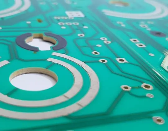
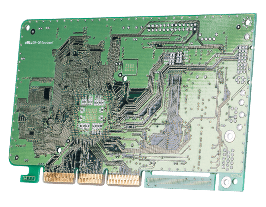
Double-sided PCBs are mainly produced on FR4 material. FR4 is a copper-clad, woven glass-reinforced material with epoxy-based resin. The epoxy resin bonds the materials together and contains flame retardants.
Product Benefits

Better Signal Integrity
DS containing both signal and ground plane layers enable better signal integrity since traces can be impedance controlled with reference in ground plane layers.

Cost-Effective
FR4 is the most cost-effective PCB material for DS PCB on the market.

High Reliability
Allow a reduction of 50% of the size of the board compared to a single-sided PCB
What is a Double-Sided PCB?
Definition
Specifications
PCB Materials: Tg. 130 to 180C°, CTE 40/220 to 60/300ppm, halogen free optionally.
Copper Weight: 1 oz/ft² minimum
Lines and Spaces: low cost 150um, standard 100um, advanced 75um
Vias: Standard 0,3mm, min. 0,15mm
Layer Count: 2-64 layers.
Surface Finish: LF HASL, OSP, Im Tin, Im Silver, ENIG, ENEPIG and Hard or Soft Gold.
Solder Mask: Green, White, Black, Blue, Red, Yellow.
Do you need Double-Sided PCB?
Double-sided PCBs are commonly used in a wide range of electronic applications such as telecommunications, industrial control systems, and power supplies. They are also used in prototyping and small-scale production runs.
Technical Data
Double-Side
| DS Feature | ICAPE Group Double Side technical specification |
|---|---|
| Technology highlights | Double side PCB with PTH (Platted Through Hole). Peelable mask, carbon ink, bevelling, countersink, edge platting. Press-fit holes +/-0,05mm. |
| Materials | FR4 raw material with high TG, high CTI, high performance and/or halogen-free. |
| Base Copper Thickness | 1/2 Oz to 15 Oz. Advanced 20 Oz |
| Minimum track & spacing | 0.1mm / 0.1mm. Advanced 0,075/0,075mm |
| Surface finishes available | OSP, HASL-LF ENIG, ENEPIG, Soft-Gold, Gold fingers, Immersion Tin, Immersion Silver. Advanced HASL. |
| Minimum mechanical drill | 0.2mm, Advanced 0,15mm |
| PCB thickness | 0.40mm – 3,2mm, Advanced 8mm. |
| Maxmimum dimensions | 530x685mm. Advanced: 1180x590mm. |
Learn more about Double-Sided PCB
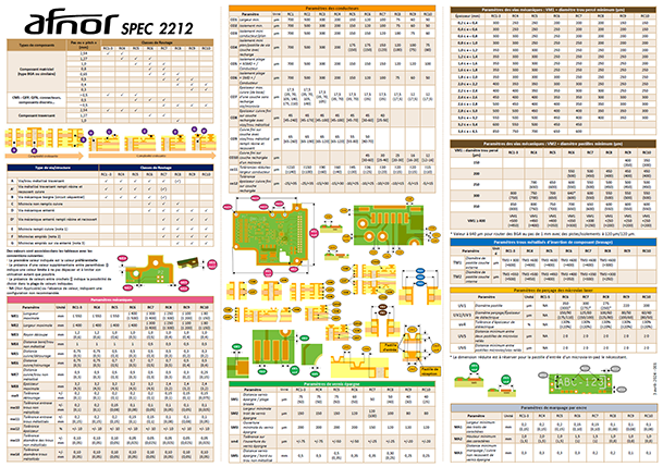
AFNOR PCB Design Guide
AFNOR SPEC 2212 is a benchmark specification developed to address the growing need for robust, sustainable, and forward-thinking solutions in PCB design

Industries
Discover how Double-sided PCB impacts several different industries and multiple fields.
Technologies
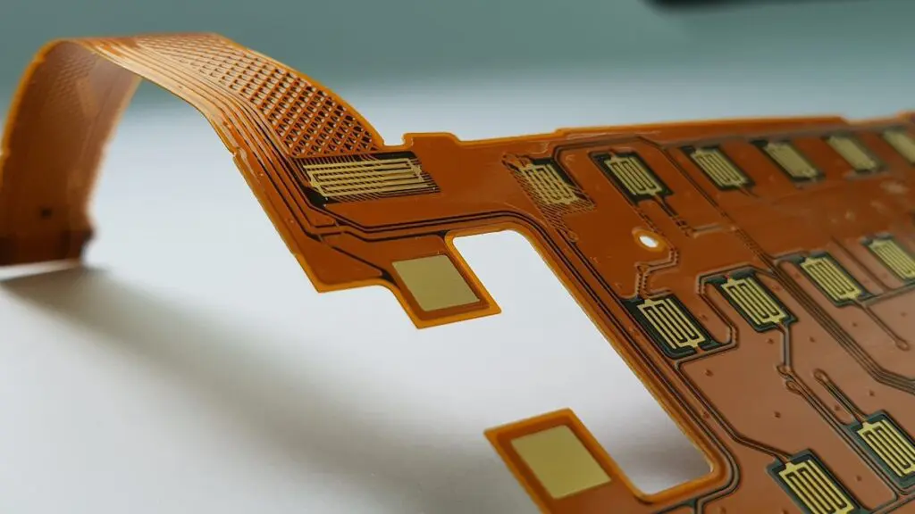
Learn about the different technologies in the PCB industry and find which one suits your needs best.
Any questions?
There is an ICAPE Group team close to you and your business. All around the world, our business units are staffed with native experts available to answer all your questions.
Contact us today!
