Ensure Quality and Standards
Compliance with Laboratory Testing
Customer Benefits

$5M Investment
Over 50 Modern Machines

6 Laboratories
in France, China, Sweden, Germany, South Africa, and the US

Bare and Assembled
Board Testing

30 Lab Technicians
With Decades of Experience
Laboratory Equipment
Between our three in-house labs, ICAPE Group has several new and modern machines that take the guesswork out of your PCB services. Below is a list of many of the machines you can find across our laboratories.
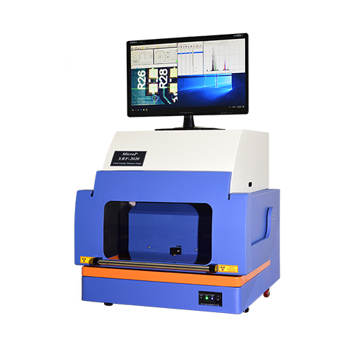
X-Ray
Fluorescence
Micro Pionner XRF 2000
To measure the thickness of multi-coating elements
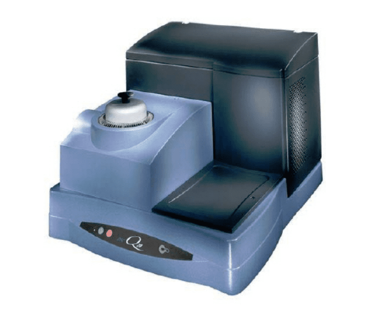
Differential Scanning Calorimeter
Ta Instruments Q20 DSC
To measure the differential heat flow
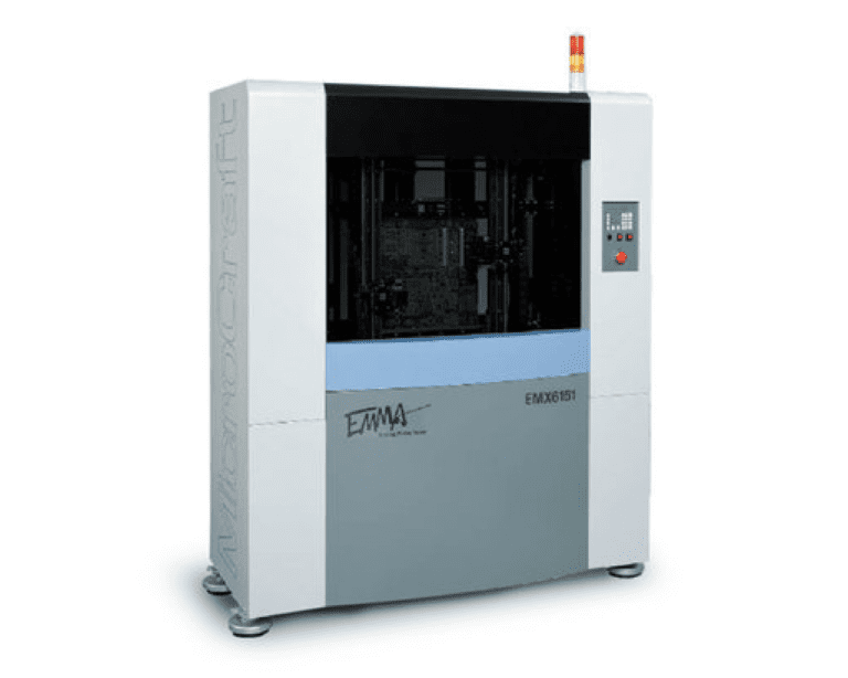
Probe Bare
Board Test
MicroCraft EMX6151 Flying
To test connectivity isolation
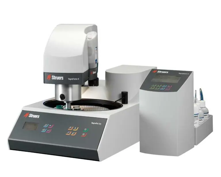
Cross
Section
Struers Micro Section System
Stuers LaboPol-20
To test cross sections
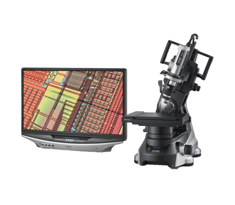
Micro Section
Analysis
Keyence VHX 7000 Microscope
To analyse micro sections
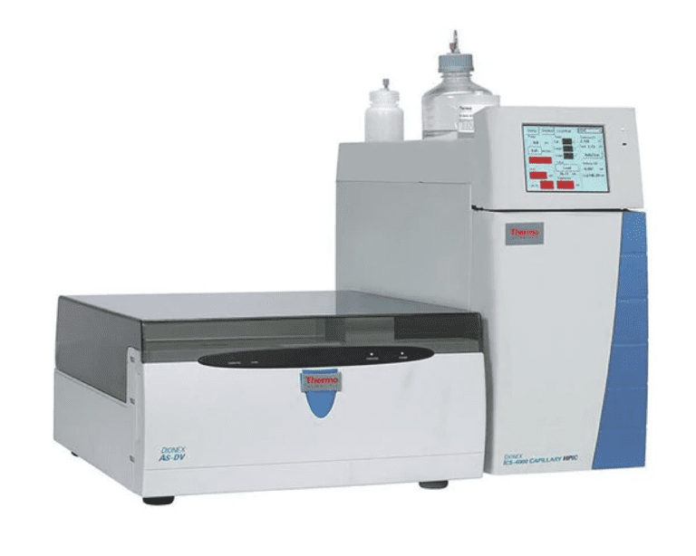
IC Separation
Dionex ICS-2100
To perform isocratic and gradient IC separations
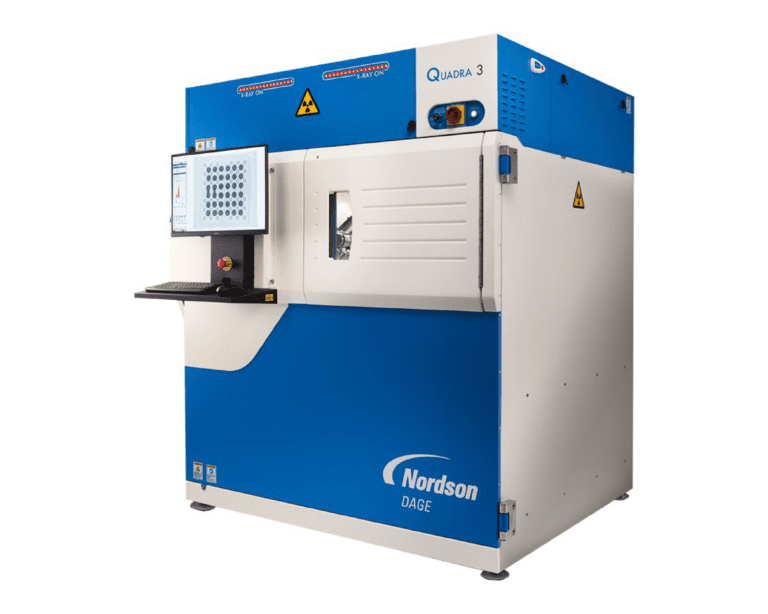
X-Ray
Inspection
Nordson Dage Quadra 3
To detect manufacturing defects
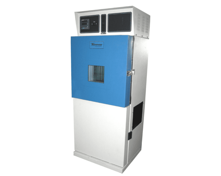
Thermal Shock
Chamber
Tenney Environmental
To test against various temperatures and humidity.
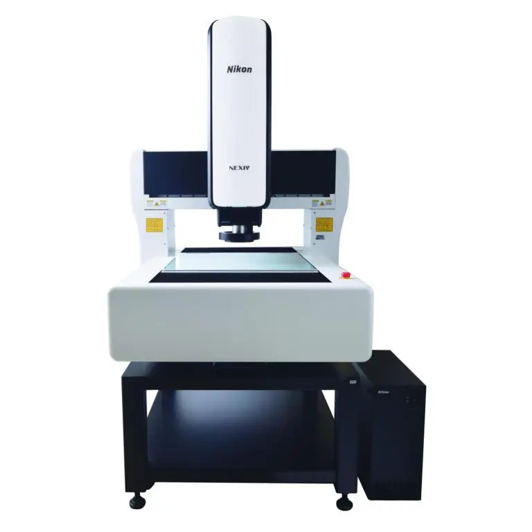
Dimensional Metrology
View Summit System
To measure large footprint parts
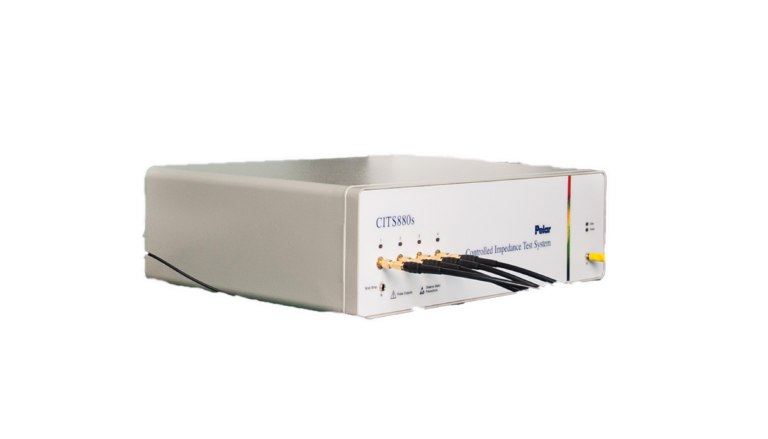
Impedance
Control
POLAR CITS880S
To check the line impedance
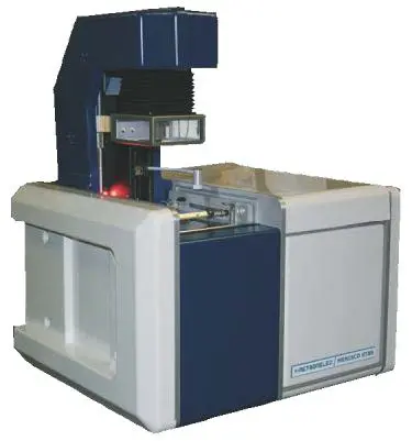
Weatting
Balance
METRONELEC ST88
To perform a solderability test
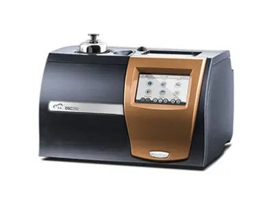
TG
Test
DICOVERY DSC25
To control the TG of the base raw material FR4
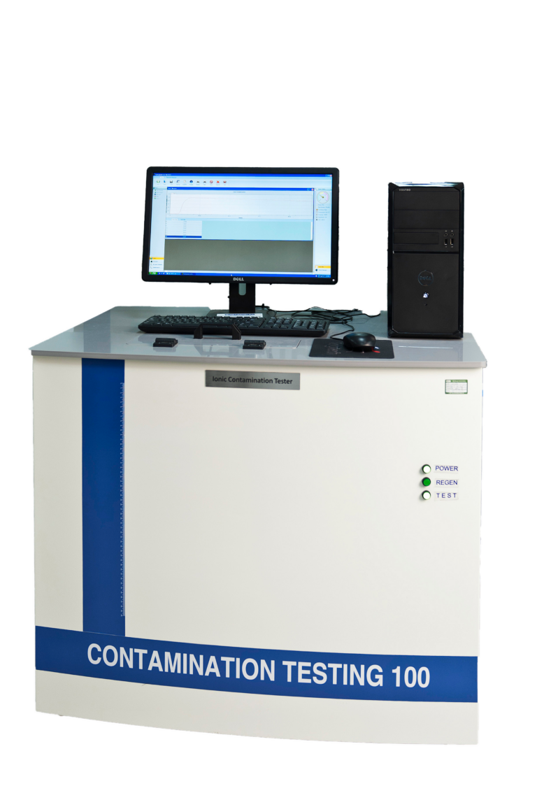
Ionic
Contamination
Metronelec
To verify the ionic contamination level
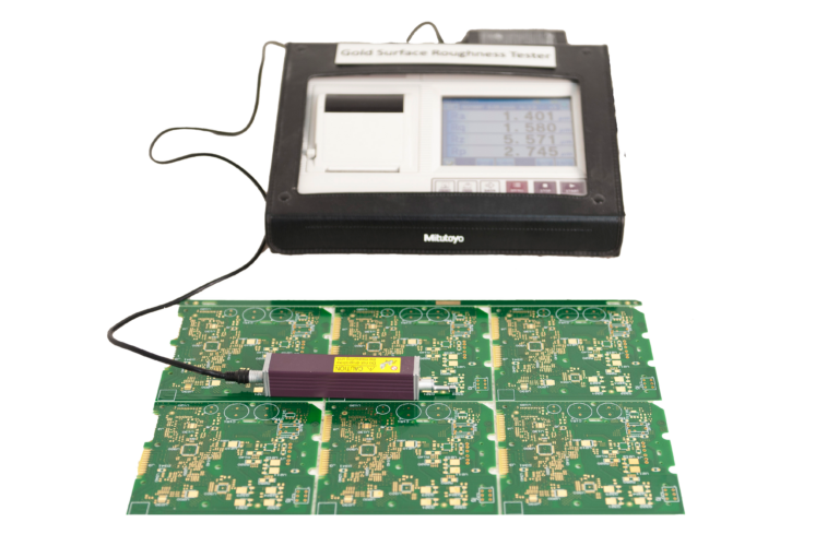
Surface
Roughness
Mitutoyo
To verify surface roughness of diverse coatings (copper, gold…)
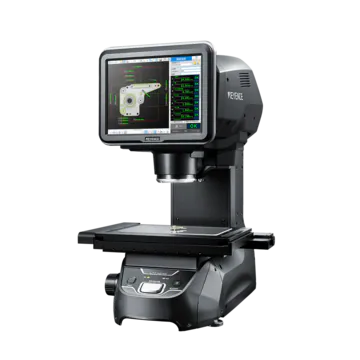
Mechanical Measurement
Keyence
To verify all geometric dimensioning
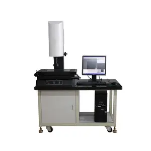
2D Semi Automatic
Measurement
Asida
To verify all geometric dimensions
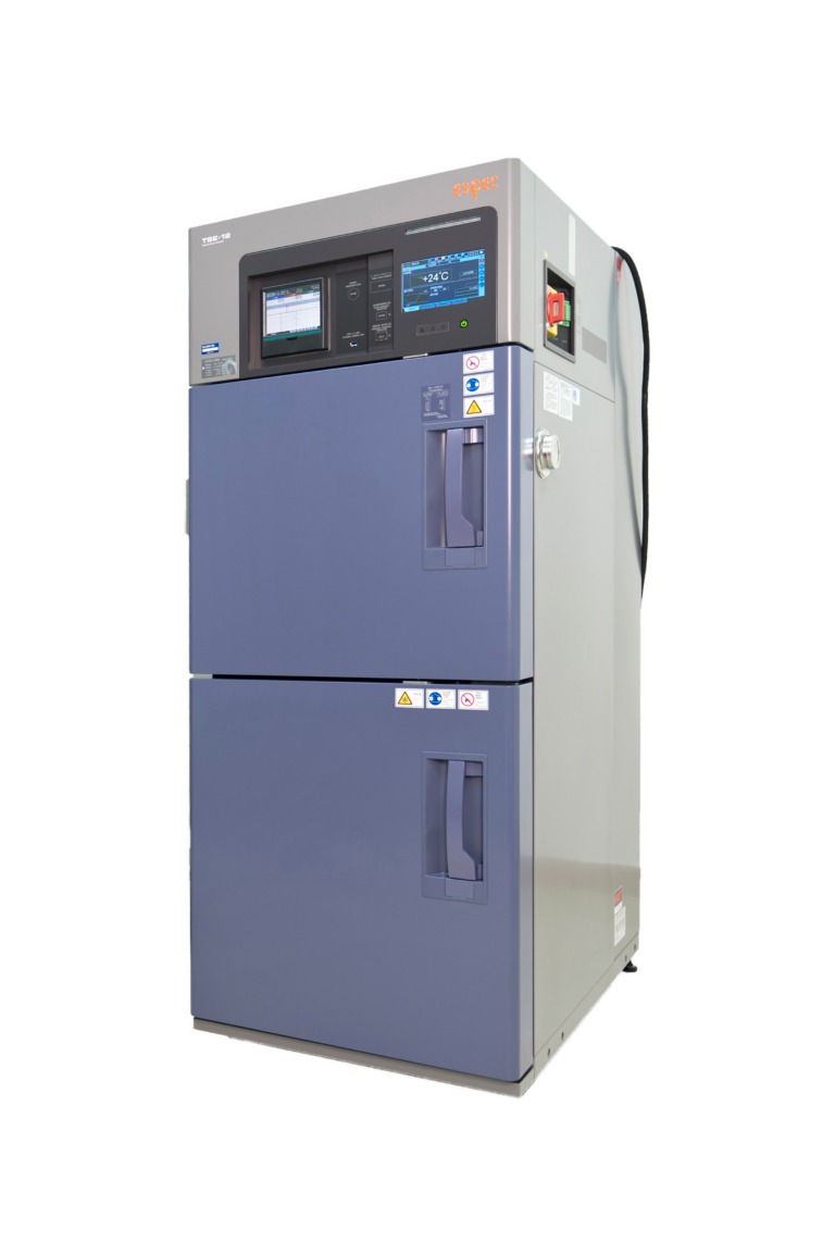
Thermal Shock
Chamber
ESPEC
To test reliability by thermal shock
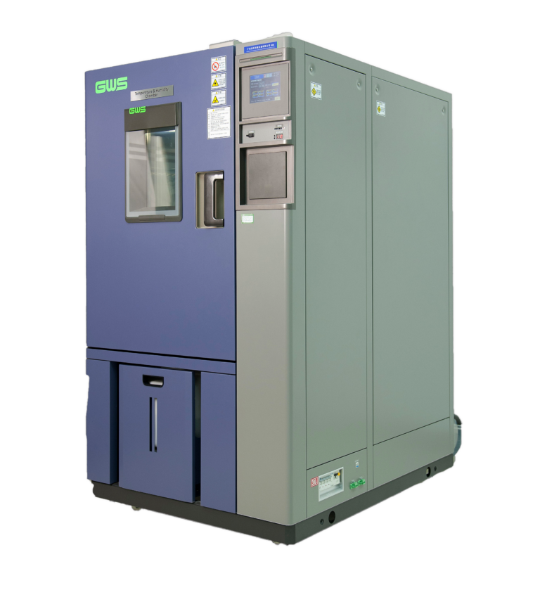
Temperature &
Humidity Chamber
GWS
To control temperature and humidity with aging test
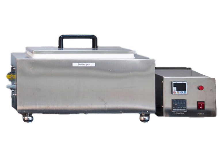
Solder
Pot
Asida
To perform thermal stress and solder float tests
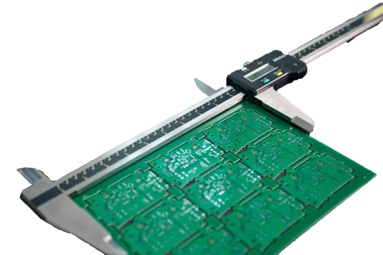
Mechanic
Measurement
Mitutoyo
To allow quality inspection
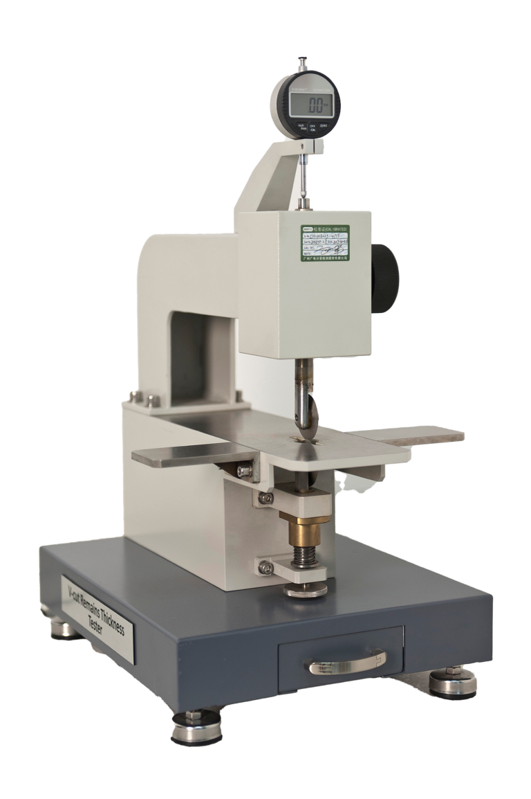
V-cut Tester
Asida
To measure the depth of V-cut
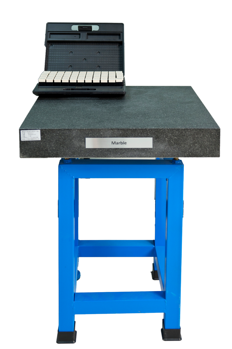
Marble
Saben
To check bow and twist
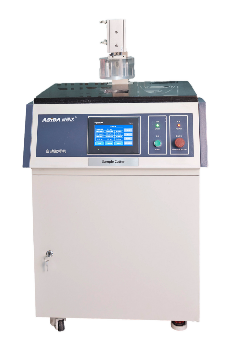
Sample Cutter
Asida
To cut various size of microsection coupon
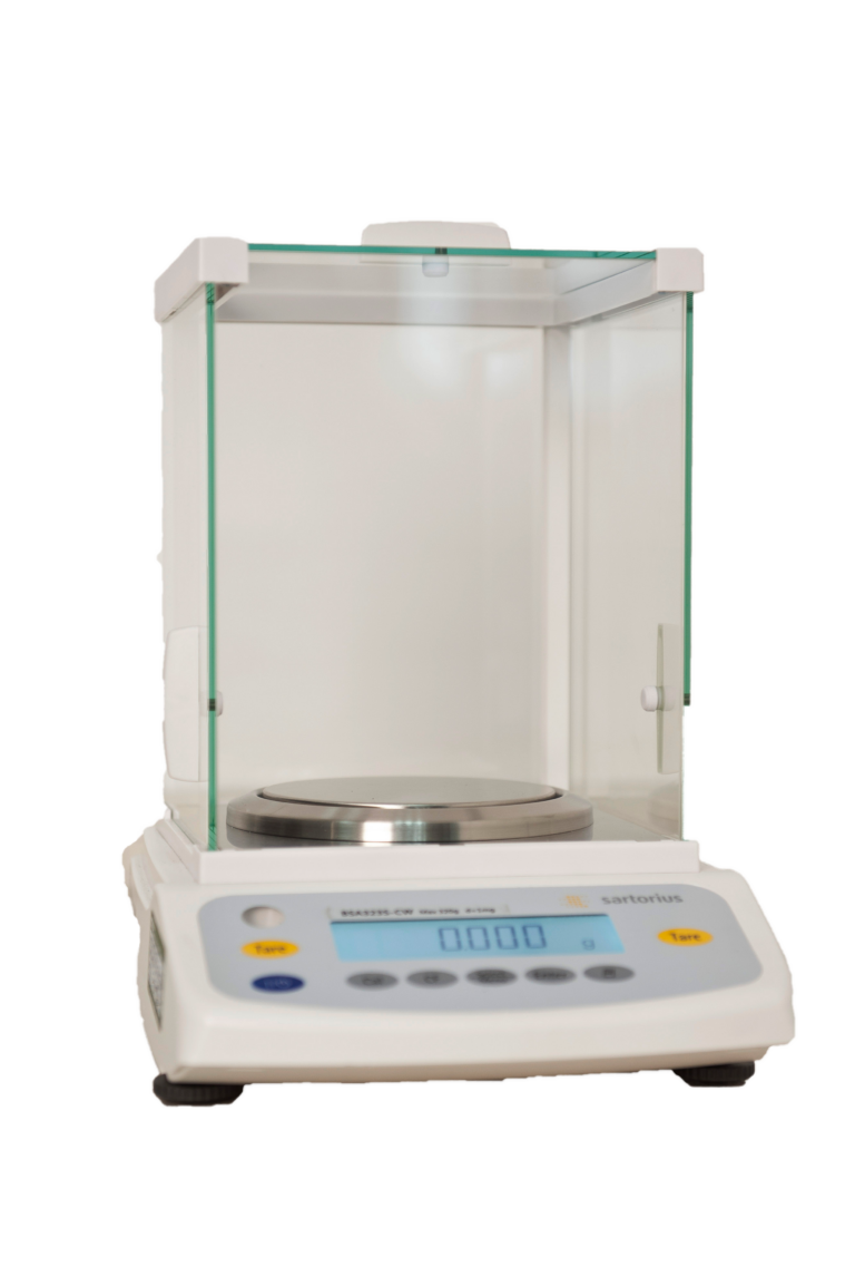
Precision
Balance
Sartotius
To measure sample weight
Lab Assurance
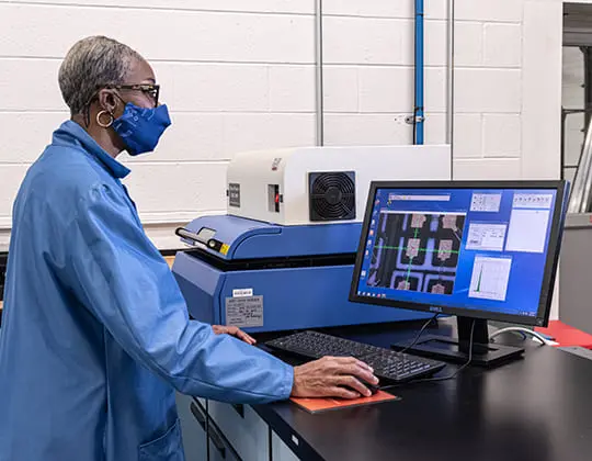
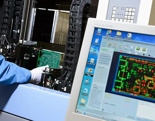
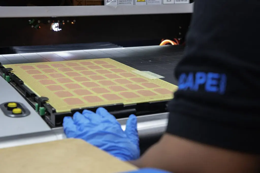
Our laboratory reports provide an “approval for use” report with the results. Our laboratory is used by customers from all industries to validate bare or assembled boards, troubleshoot problems, or verify their boards.
Industry Expertise
Laboratory Tests
Risk-free
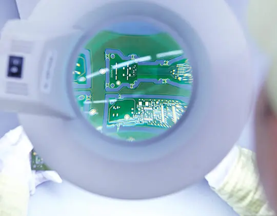
The surface mount technology (SMT) process utilizes barcode component verification at placement for passive component validation and AOI (Automated optical inspection) to enable a fast and accurate review of your PCB/A.
